Titanium Oxide Nanostructuring Enables Precise Formation on Metal Coatings, Pushing Boundaries

Precisely formed large metal surfaces coated with nanostructures have so far remained in the realm of fantasy. The obstacle to their production seemed fundamental, as it stemmed from the presence of crystal grains in metals, whose boundaries disrupted the growth of nanostructures. At the Institute of Nuclear Physics of the Polish Academy of Sciences, using titanium and its oxide as an example, it has been demonstrated that this obstacle can be overcome.
Large metal surfaces coated with precisely engineered nanostructures have remained in the realm of fantasy until now. The obstacle to their production appeared fundamental, arising from the presence of crystal grains in metals; their boundaries disrupted the growth of nanostructures. At the Institute of Nuclear Physics of the Polish Academy of Sciences, using titanium and its oxide as examples, it has been demonstrated that this barrier can be overcome.
Coatings made from nanostructures with precisely selected dimensions and shapes allow control of material properties. Unfortunately, in most metals there was a serious limitation: due to disturbances occurring at crystal grain boundaries, it was impossible to produce homogeneous coatings on large surfaces.
This limitation was overcome at the Institute of Nuclear Physics of the Polish Academy of Sciences (IFJ PAN) in Kraków, and using titanium and its oxide as examples, a large-area metal coating process with nanotubes was demonstrated. This success appears promising in the context of many applications including medical implants, photovoltaic cells, chemical detectors, and memristors.
"Uniquely in the world, we have the ability to coat large titanium sheet areas measuring dozens of square centimeters with titanium oxide nanotubes in a precisely controlled manner. Our proposed method is the result of combining two unconventional techniques for nanostructuring material surfaces: nanoparticle lithography and electrochemical anodization," says Dr. Eng. Juliusz Chojenka (IFJ PAN), the lead author of the article explaining the success published in Acta Materialia.
Both nanoparticle lithography and anodization have been known techniques for a long time, but have only been used at laboratory scale and have not been combined until now. The physicists from Kraków emphasize that the advantage of the proposed methods is simplicity, speed, low manufacturing costs, and the possibility of easily scaling up the entire process to allow technological applications such as producing large-area coatings.
Nanoparticle lithography plays a role in the first, preparatory stage of producing titanium oxide nanotube coatings. The main actors here are commercially available spherical polystyrene nanoparticles ranging in size from 50 nanometers to several dozen micrometers. Nanospheres of the selected size are added to water in quantities that will form a single layer of the desired thickness when floating on the surface. Since the nanoparticles become electrically charged during this process, they repel each other, resulting in uniform distribution characterized by hexagonal regularity.
The extremely uniform single layer of polystyrene nanoparticles is then placed on a polished titanium sheet. The material coated with nanoparticles is now placed in a vacuum chamber where it is exposed for several minutes to plasma generated from nitrogen and oxygen. Under its effect, the polystyrene spheres shrink slightly but retain their original positions. The sample is then transferred to another vacuum chamber where a thin layer of titanium is deposited on it.
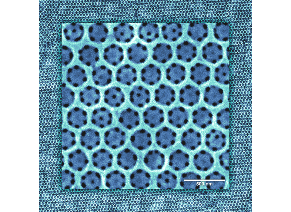
The final stage of the lithographic phase involves removal of the nanoparticles using organic solvent and ultrasound, which causes the sample to vibrate. The result is a surface covered with a hexagonal, regular cavity network called antidots.
"In a special chamber, we now subject the sample coated with antidots to anodization, an electrochemical process that results in the formation of uniform and regular nanostructures on the surface," explains Dr. Eng. Michal Krupinski (IFJ PAN).
"By cleverly selecting the electrolyte composition in which anodization occurs and controlling the applied voltage, temperature, and time, we can create a dense titanium oxide nanotube coating arranged according to the original antidot pattern and of a predetermined length—in the case explained in our paper, 15 micrometers.
It should be emphasized here that standard titanium anodization is subject to serious physical limitations regarding the regularity scale of nanostructures resulting from the size of crystal grains in the metal matrix. For this reason, the physicists in Kraków apply a nanopatterning process using nanoparticle lithography before anodization. Lithography, by allowing modification of the electric field distribution on the titanium surface, which is important during anodization, forces long-range ordering of the resulting nanostructures.
The physical and chemical properties of coatings obtained in this way were characterized comprehensively using scanning electron microscopy, X-ray diffraction, and Raman spectroscopy, and their photoactivity under ultraviolet radiation was also determined. During several days of testing, it was found that the nanotube coatings produced, despite crossing crystal grain boundaries, were mechanically durable and the nanotubes themselves did not fracture even during annealing.
The presented titanium oxide nanostructuring method has broad application potential. Medical implants can be coated with nanotubes that increase biocompatibility and controllably release medications into the body.
By skillfully selecting the size and density of nanotubes, it is possible to control the photoactivity of titanium oxide interacting with ultraviolet radiation, which promotes applications related to photovoltaic cells or control of chemical reactions. It is also known that the properties of the titanium oxide surface change depending on minimal hydrogen adsorption, so new detectors more sensitive than those currently available are also being considered.
Interesting perspectives emerge in the miniaturization of memristors, electronic components whose resistance depends on the history of current passing through them. Currently, memristors, which are promising components of new types of memory and artificial synapses, are on the order of tens of micrometers in size. Meanwhile, their functions can be performed by individual nanotubes, which are at least a hundred times smaller.
"There is no physical, chemical, or technical barrier to adapting our method to nanostructuring of surfaces made from transition metals such as iron, aluminum, or tantalum other than titanium. Everything depends on the requirements," concludes Dr. Chojenka.
Gallery